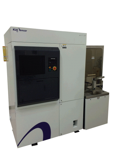
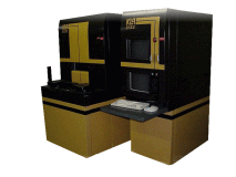
- Equipment configuration:
- High-throughput scanning for patterned wafer inspection
- Product Description
- Adjusts dynamically to all die regions to deliver maximum sensitivity and improved detection of killer defects in a single scan, regardless of pattern density.
- Features faster recipe setup, fewer setup parameters, improved recipe robustness, and user-friendly setup templates.
- Enables improved cost of ownership through use of larger spot sizes with similar sensitivity results.
- Extends a fab's inspection capability while leveraging existing learning and capital investment in the AIT II and AIT III.
- Enables process monitoring and copper CMP inspection through enhanced signal-to-noise and nuisance filtering.
加入詢問單
TOP